


A formulation of methylammounium iodide (MAI), PbCl2 and PbI2 at a molar ratio of 1:1:4 (PbCl2:PbI2:MAI) in a DMF solvent. On processing, I201 ink can be used to create a CH3NH3PbI3-xClx perovskite film. The process recipe for I201 is optimised for glove box processing under a nitrogen atmosphere.
I201 perovskite ink is divided into 10 lots of 0.5 ml. We have found this quantity to be sufficient for 10 individual experiments (approximately 160 device substrates).
Datasheet
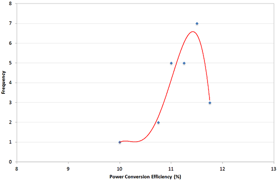
We have specially formulated I201 Perovskite Ink in our laboratories to make it suitable for deposition by spin-coating. It is based on similar ink formulations used in references [1]. This ink is designed to be used with a bottom ITO/PEDOT:PSS anode and a top PC70BM/Ca/Al cathode, with PV devices fabricated with an average / peak power conversion efficiency (PCE) of (11.2% ± 0.4)% / 11.8%. This performance level is in accord with other literature reports using similar ink formulations where PCEs of approximately 11.5% have been demonstrated [1]. A full process recipe comes with the ink, which is ready to use after heating for a short time.

References (please note that Ossila has no formal connection to any of the authors or institutions in these references):
- Reproducible One-Step Fabrication of Compact MAPbI3-xClx Thin Films Derived from Mixed-Lead-Halide Precursors, D. Wang et al., Chem. Mater., 26, 7145-7150 (2014) DOI: 10.1021/cm5037869
Specifications
Perovskite precursor ink formulation: Ink I201 is based on a mixture of methylammonium iodide (MAI), lead chloride (PbCl2) and lead iodide (PbI2) at a molar ratio (PbCl2:PbI2:MAI) of 1:1:4 dissolved in anhydrous DMF (dimethylformamide).
| Compound | Purity | Molar Ratio |
|---|---|---|
| MAI | > 99% (as measured by Elemental Analysis) | 1 |
| PbCl2 | 99.999% | 1 |
| PbI2 | 99.999% | 4 |
| DMF | 99.8% | n/a |
Now selling bulk orders of 30ml with a 25% discount over our standard order sizes.

Usage Details
Fabrication Routine for Perovskite Precursor Ink I201
Glass / ITO / PEDOT:PSS / CH3NH3PbI3-xClx / PC70BM / Ca / Al
For complete step-by-step instructions please see our Full Perovskite Solar Cells Fabrication Video or written fabrication guide. Please note, however, that the routine in these full guides differs slightly to the optimised routine for the I201, which is designed to be processed in a nitrogen filled glove box.
The summary below outlines the key steps required when processing I201 ink. You can also download this summary as a PDF in order to print and laminate it for us in a clean room.
1. Substrate clean (in air):
- Sonicate ITO substrates for 5 minutes in hot (70°C) 1% Hellmanex
- Dump-rinse substrates twice in boiling, deionised (DI) water
- Sonicate for 5 mins in IPA. Dump-rinse twice in boiling DI water
- Dry the substrates with nitrogen gun
- Bake the substrates on a hotplate at 120°C.
2. PEDOT:PSS anode preparation (in air):
- Filter AI 4083 PEDOT:PSS using a 0.45 µm PES filter
- Dispense 35 µl of the filtered PEDOT:PSS solution onto the heated ITO substrate spinning at 6000 rpm for 30s
- Place substrate onto a hotplate at 120°C
- After all ITO substrates have been coated with a PEDOT:PSS layer, transfer all to a nitrogen-filled glove box and place onto a hotplate at 120°C for 20-30 mins
- Remove the substrates from the hotplate and allow to cool at room temperature.
3. Perovskite deposition (in nitrogen glove box):
- Heat I201 ink for 2 hours at 70°C and then cool to room temperature
- Place the ITO coated substrate (at room temperature) onto the spin-coater and spin the substrate at 4000 rpm (for 30s)
- Dynamically dispense 30 µl of I201 ink
- Place substrate back onto the hotplate (in the glove box) at 80°C
- Once all substrates have been coated, anneal for 90 mins
- After 90 mins, use a cleaning swab dipped in a small amount of DMF solvent to wipe the cathode stripe clean
- After cleaning, anneal for an addition 20-30 mins at 80°C to remove any residual DMF solvent
- After this time, remove substrates from the hotplate and cool to room temperature.
4. PC70BM deposition (in nitrogen glove box):
- Prepare a solution of PC70BM at 50 mg / ml in chlorobenzene and stir for 3 to 5 hours
- Place perovskite coated substrate onto the spin-coater and spin at 1000 rpm
- Dispense 20 µl of PC70BM solution onto the substrate (while spinning) and spin for a total time of 30s.
5. Cathode deposition:
- Thermally evaporate a calcium/aluminium cathode (5 and 100 nm respectively) through shadow-mask
- Encapsulate devices using a glass coverslip and encapsulation epoxy
- Expose to UV radiation (350 nm) for 30 mins to cure epoxy.
Perovskite Photovoltaic Device Performance
Below are device characteristics for our best pixel fabricated using the I201 fabrication recipe described above.
JV curves demonstrate the hysteresis observed from the device and include device metrics for both forward and reverse sweeps. The pixel presented (from a reverse sweep) had a power conversion efficiency of 11.8%, a Voc of 0.91 V, a FF of 79% and a Jsc of -16.5 mA/cm2.

To the best of our knowledge the technical information provided here is accurate. However, Ossila assume no liability for the accuracy of this information. The values provided here are typical at the time of manufacture and may vary over time and from batch to batch.
About Ossila Founded in 2009 by organic electronics research scientists, Ossila aims to provide the components, equipment, and materials to enable intelligent and efficient scientific research and discovery. Over a decade on, we're proud to supply our products to over 1000 different institutions in over 80 countries globally. With decades of academic and industrial experience in developing organic and thin-film LEDs, photovoltaics, and FETs, we know how long it takes to establish a reliable and efficient device fabrication and testing process. As such, we have developed coherent packages of products and services - enabling researchers to jump-start their organic electronics development program. The Ossila Guarantee Free Worldwide Shipping Eligible orders ship free to anywhere in the world Fast Secure Dispatch Rapid dispatch on in-stock items via secure tracked courier services Quality Assured Backed up by our free two year warranty on all equipment Clear Upfront Pricing Clear pricing in over 30 currencies with no hidden costs Large Order Discounts Save 8% on orders over $10,300.00 and 10% on orders over $12,900.00 Expert Support Our in-house scientists and engineers are always ready to help Trusted Worldwide Great products and service. Have already recommended to many people. Dr. Gregory Welch, University of Calgary Wonderful company with reasonably priced products and so customer-friendly! Shahriar Anwar, Arizona State University The Ossila Team Prof. David Lidzey - Chairman As professor of physics at the University of Sheffield, Prof. David Lidzey heads the university’s Electronic and Photonic Molecular Materials research group (EPMM). During his career, David has worked in both academic and technical environments, with his main areas of research including hybrid organic-inorganic semiconductor materials and devices, organic photonic devices and structures and solution processed photovoltaic devices. Throughout his academic career, he has authored over 220 peer-reviewed papers. Dr. James Kingsley - Managing Director James is a co-founder and managing director of Ossila. With a PhD in quantum mechanics/nanotech and over 12 years’ experience in organic electronics, his work on the fabrication throughput of organic photovoltaics led to the formation of Ossila and the establishment of a strong guiding ethos: to speed up the pace of scientific discovery. James is particularly interested in developing innovative equipment and improving the accessibility of new materials for solution-processable photovoltaics and hybrid organic-inorganic devices. Dr. Alastair Buckley - Technical Director Alastair is a lecturer of Physics at the University of Sheffield, specialising in organic electronics and photonics. He is also a member of the EPMM research group with a focus on understanding and applying the intrinsic advantages of functional organic materials to a range of optoelectronic devices. Alastair’s experience has not been gained solely in academia; he previously led the R&D team at MicroEmissive Displays and therefore has extensive technical experience in OLED displays. He is also the editor and contributor of "Organic Light-Emitting Diodes" by Elsevier. Our Research Scientists Our research scientists and product developers have significant experience in the synthesis and processing of materials and the fabrication and testing of devices. The vision behind Ossila is to share this experience with academic and industrial researchers alike, and to make their research more efficient. By providing products and services that take the hard work out of the device fabrication process, and the equipment to enable accurate, rapid testing, we can free scientists to focus on what they do best - science. Customer Care Team The customer care team is responsible for the customer journey at Ossila. From creating and providing quotes, through to procurement and inventory management, the customer care team is devoted to providing first class customer service. The general day to day responsibilities of a customer care team member involves processing customers orders and price queries, answering customer enquiries, arranging the shipment of parcels and notifying customers of updates on their orders. Collaborations and Partnerships Please contact the customer care team for all enquires, including technical questions about Ossila products or for advice on fabrication and measurement processes. Location and Facilities Ossila is based at the Solpro Business Park in Attercliffe, Sheffield. We operate a purpose-built synthetic chemistry and device testing laboratory on site, where all of our high-purity, batch-specific polymers and other formulations are made. This is complemented by a dedicated suite of thin-film and organic electronics testing and analysis tools within the device fabrication cluster housed in a class 1000 cleanroom in the EPSRC National Epitaxy Facility in Sheffield. All our electronic equipment is manufactured on-site.
