


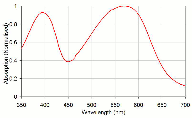
PCDTBT is one of the next generation donor materials developed for organic photovoltaics to produce better efficiencies and lifetimes. The key properties of PCDTBT result from the lower HOMO/LUMO levels which lead to advantages over standard organic photovoltaic materials of increased open circuit voltage, longer wavelength absorption and improved stability under ambient conditions.
The lower lying HOMO level of PCDTBT makes it much more stable under ambient conditions and therefore an ideal candidate to use with large area deposition methods such as ink-jet printing, spray coating and blade coating. However, for these deposition techniques, uniform, aggregate free coatings are essential and so lower molecular weights are often desirable.
Power conversion efficiencies of up to 6.7% have been achieved in our own labs using PCDTBT (M137) in a standard reference architecture using PEDOT:PSS as a hole interface and calcium/aluminium as an electron interface. By using advanced interface materials and antireflection coatings PCDTBT has also achieved up to 7.2% in the literature [1].
For information on processing please see our specific fabrication details for PCDTBT below, general fabrication video, general fabrication guide, optical modelling paper on our standard architecture [2], or email us for any additional help and support.
Luminosyn™ PCDTBT
Luminosyn™ PCDTBT is now available.
High efficiencyPower conversion efficiencies of up to 6.7% having been achieved in our own lab
High purityPCDTBT is purified by soxhlet extraction with methanol, hexane and chlorobenzene under argon atmosphere
Batch-specific GPC dataHave confidence in what you are ordering; batch-specific GPC data for your thesis or publications
Large quantity ordersPlan your experiments with confidence with polymers from the same batch
General Information
| Full name | Poly[N-9"-heptadecanyl-2,7-carbazole-alt-5,5-(4",7"-di-2-thienyl-2",1",3"-benzothiadiazole)] |
| Synonyms | PCDTBT |
| CAS number | 958261-50-2 |
| Chemical formula | (C43H47N3S3)n |
| Molecular weight | See Batch Details for information |
| HOMO / LUMO | HOMO = -5.4 eV, LUMO = -3.6 eV |
| Solubility | Chloroform, chlorobenzene, dichlorobenzene and trichlorobenzene |
| Classification / Family | Polycarbazoles, Heterocyclic five-membered ring, Organic semiconducting materials, Low band gap polymers, Organic photovoltaics, Polymer solar cells, OLEDs, OFETs and Perovskite solar cells |
Chemical Structure

Usage Datasheet
For high performance organic photovoltaics with efficiencies of 6% and above poly[N-9"-heptadecanyl-2,7-carbazole-alt-5,5-(4",7"-di-2-thienyl-2",1",3"-benzothiadiazole)] (PCDTBT). We have achieved efficiencies of 6.7% in our own labs using a standard reference architecture of PEDOT:PSS as a hole interface and calcium/aluminium as an electron interface (see below for fabrication details). Our paper published in Nature Scientific Reports titled Molecular weight dependent vertical composition profiles of PCDTBT:PC71BM blends for organic photovoltaics explores the effect and optimisation of molecular weight.


Solution Details
Ossila’s reference devices were made by dissolving PCDTBT (M137) at 4 mg/ml in anhydrous chlorobenzene using a stir-bar and hotplate at 80°C overnight. This was then mixed with Ossila’s dry 95%/5% C70 PCBM (M113) powder in a 1:4 blend ratio to produce an overall concentration of 20 mg/ml.The blend solution was heated with a stir-bar on a hotplate at 80°C for 2 hours before cooling to room temperature over 10 minutes and filtering with a 0.45 μm PTFE filter immediately prior to spinning at 700 rpm to give a film of approx. 70 nm.
Device Structure
Glass / ITO / PEDOT:PSS / PCDTBT:PC70BM / Ca / Al
Ossila’s pre-patterned ITO substrates (S171) with 100 nm (20 Ω/square) ITO were cleaned with the following procedure:
- 5 minutes sonication in hot 1% Hellmanex III
- 2x hot dump rinses, 1x cold dump rinse
- 5 minutes sonication in warm IPA
- 3x cold dump rinses
- 5 minutes sonication in hot 10% NaOH solution
- 2x cold dump rinses then stored in DI water until use
- N2 blow dry before spin-coating the hole transport layer (no further cleaning or surface treatment required)
PEDOT:PSS (AI4083 from Ossila) was filtered through a 0.45 µm PES filter (C2009S1) before spin coating at 6000 rpm in air to produce a layer 30 nm thick. The coated substrates were then stored on a hotplate at 150°C before transfer into a glove box and a further bake of 150°C for 10 mins to remove any residual moisture.The active ink was spin cast and the cathode strip wiped clean using chlorobenzene before transfer to an evaporator where 2.5 nm of Ca followed by 100 nm of Al were deposited at <10-6 mbar. The substrates were then annealed at 80°C for 15 mins on a hotplate in the glove box before protecting with the Ossila encapsulation system. Measurement was performed under ambient conditions using a Newport 92251A AM1.5 100 mW/cm2 solar simulator and NREL certified silicon reference cell.
As Featured In...

All-Inkjet-Printed, All-Air-Processed Solar Cells, Sirringhaus, McNeill et al., Advanced Energy Materials, 1400432, 2014
"Our in depth study on PCDTBT:PC70BM layers demonstrated that inkjet-printed blend layers exhibited similar nanoscale structure and excited state dynamics to spin-coated layers."
MSDS Documentation
 PCDTBT MSDS sheet
Pricing
| Batch | Quantity | Price |
| M1311 | 100 mg | £198.00 |
| M1311 | 250 mg | £396.00 |
| M1311 | 500 mg | £677.00 |
| M1311 | 1 g | £1090.00 |
| M1311 | 2 g | £1990.00 |
| M1311 | 5 g / 10 g* | Please enquire |
*for 5 - 10 grams order quantity, the lead time is 4-6 weeks.
Batch Details
The below materials are in stock for immediate dispatch to research institutions worldwide.
In general, PCDTBT is used at lower concentrations than P3HT (typically 4 to 7 mg/ml) and higher blend ratios (1:4 PCDTBT:PC70BM) and as such 100 mg of PCDTBT will make around 500 devices on Ossila"s standard ITO substrates (20 x 15 mm) even assuming 50% material loss in filtration and solution preparation. Please note that as the higher molecular weight fractions have a lower yield we are now operating differential pricing policy. See below for more details on separation, yield and differential pricing.
| Batch | Mw | Mn | PDI | Stock Info |
| M1311 | 34,900 | 16,200 | 2.15 | In stock |
Literature and References
Please note that Ossila has no formal connection to any other authors or institutions in these references.
- Efficient, Air-Stable Bulk Heterojunction Polymer Solar Cells Using MoOx as the Anode Interfacial Layer, Y. Sun et al., Advanced Materials, 23, 2226-2230 (2011)
- Optimising the efficiency of carbazole co-polymer solar-cells by control over the metal cathode electrode, D.C. Watters et al., Organic Electronics, 13, 1401-1408 (2012)
- Efficient perovskite photovoltaic devices using chemically doped PCDTBT as a hole-transport material, M. Wong-Stringer et al., J. Mater. Chem. A, 2017, 5, 15714-15723; DOI: 10.1039/C7TA03103C.
To the best of our knowledge the technical information provided here is accurate. However, Ossila assume no liability for the accuracy of this information. The values provided here are typical at the time of manufacture and may vary over time and from batch to batch.
About Ossila Founded in 2009 by organic electronics research scientists, Ossila aims to provide the components, equipment, and materials to enable intelligent and efficient scientific research and discovery. Over a decade on, we're proud to supply our products to over 1000 different institutions in over 80 countries globally. With decades of academic and industrial experience in developing organic and thin-film LEDs, photovoltaics, and FETs, we know how long it takes to establish a reliable and efficient device fabrication and testing process. As such, we have developed coherent packages of products and services - enabling researchers to jump-start their organic electronics development program. The Ossila Guarantee Free Worldwide Shipping Eligible orders ship free to anywhere in the world Fast Secure Dispatch Rapid dispatch on in-stock items via secure tracked courier services Quality Assured Backed up by our free two year warranty on all equipment Clear Upfront Pricing Clear pricing in over 30 currencies with no hidden costs Large Order Discounts Save 8% on orders over $10,300.00 and 10% on orders over $12,900.00 Expert Support Our in-house scientists and engineers are always ready to help Trusted Worldwide Great products and service. Have already recommended to many people. Dr. Gregory Welch, University of Calgary Wonderful company with reasonably priced products and so customer-friendly! Shahriar Anwar, Arizona State University The Ossila Team Prof. David Lidzey - Chairman As professor of physics at the University of Sheffield, Prof. David Lidzey heads the university’s Electronic and Photonic Molecular Materials research group (EPMM). During his career, David has worked in both academic and technical environments, with his main areas of research including hybrid organic-inorganic semiconductor materials and devices, organic photonic devices and structures and solution processed photovoltaic devices. Throughout his academic career, he has authored over 220 peer-reviewed papers. Dr. James Kingsley - Managing Director James is a co-founder and managing director of Ossila. With a PhD in quantum mechanics/nanotech and over 12 years’ experience in organic electronics, his work on the fabrication throughput of organic photovoltaics led to the formation of Ossila and the establishment of a strong guiding ethos: to speed up the pace of scientific discovery. James is particularly interested in developing innovative equipment and improving the accessibility of new materials for solution-processable photovoltaics and hybrid organic-inorganic devices. Dr. Alastair Buckley - Technical Director Alastair is a lecturer of Physics at the University of Sheffield, specialising in organic electronics and photonics. He is also a member of the EPMM research group with a focus on understanding and applying the intrinsic advantages of functional organic materials to a range of optoelectronic devices. Alastair’s experience has not been gained solely in academia; he previously led the R&D team at MicroEmissive Displays and therefore has extensive technical experience in OLED displays. He is also the editor and contributor of "Organic Light-Emitting Diodes" by Elsevier. Our Research Scientists Our research scientists and product developers have significant experience in the synthesis and processing of materials and the fabrication and testing of devices. The vision behind Ossila is to share this experience with academic and industrial researchers alike, and to make their research more efficient. By providing products and services that take the hard work out of the device fabrication process, and the equipment to enable accurate, rapid testing, we can free scientists to focus on what they do best - science. Customer Care Team The customer care team is responsible for the customer journey at Ossila. From creating and providing quotes, through to procurement and inventory management, the customer care team is devoted to providing first class customer service. The general day to day responsibilities of a customer care team member involves processing customers orders and price queries, answering customer enquiries, arranging the shipment of parcels and notifying customers of updates on their orders. Collaborations and Partnerships Please contact the customer care team for all enquires, including technical questions about Ossila products or for advice on fabrication and measurement processes. Location and Facilities Ossila is based at the Solpro Business Park in Attercliffe, Sheffield. We operate a purpose-built synthetic chemistry and device testing laboratory on site, where all of our high-purity, batch-specific polymers and other formulations are made. This is complemented by a dedicated suite of thin-film and organic electronics testing and analysis tools within the device fabrication cluster housed in a class 1000 cleanroom in the EPSRC National Epitaxy Facility in Sheffield. All our electronic equipment is manufactured on-site.