
The Ossila pre-patterned ITO OFET and sensing substrates have been designed to enable the fabrication and characterisation of transistors and sensing devices without the need for vacuum evaporations or probe stations. This allows devices to be produced and tested with significantly increased simplicity, making the system ideal for reducing costs of material screening experiments; as well as teaching and training purposes.
Specifications
| Substrate size | 20 mm x 15 mm |
| Pack size | 100 substrates per standard pack |
| Thickness | 1.1 mm |
| Channel dimensions | S161: W × L: 30 mm × 50 μm S162: W × L: 30 mm × 50, 75, 100, 150 and 200 μm |
| Glass type | Polished soda lime, float glass |
| Substrate coating | Fully oxidised ITO |
| ITO thickness | 100 nm |
| ITO resistance | 20 Ω / square |
| Glass roughness | < 1 nm RMS (By AFM) |
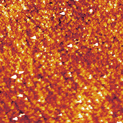
| ITO roughness | 1.8 nm RMS (By AFM) |
The pre-patterned OFET substrates consist of interdigitated ITO fingers to act as the source-drain electrodes, and have overall channel dimensions of 30 mm x 50 μm. These relatively large channels work to minimise contact effects, so it is less important to match the energy levels of the organic semiconductor and contacts. As such, the intrinsic Poole Frenkel limited mobility of a material can be more easily assessed independent of the HOMO level. The 30 mm channel width also has the additional benefit of producing larger currents, making testing and measurement quicker and requiring less sensitive (and less expensive) equipment.
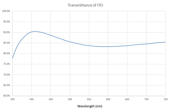
The substrate itself is made of high-quality soda-lime float glass with a 20 nm coating of SiO2 (synthetic quartz). The transparent nature of the ITO/glass also means that opto-electric experiments can be done with ease (photoconductivity, photo-induced doping in the presence of oxygen, sensing).
Transistors can be fabricated by simply depositing an organic semiconductor, gate insulator and gate on the substrates (see diagram below for device schematic). By using a synthetic metal (such as PEDOT:PSS) deposited from solution for the gate, it is possible to make fully-functioning OFETs by solution processing alone, eliminating vacuum evaporation processes. The use of the Ossila OFET test board also means that devices can be measured at the flick of a switch without the need for probe stations.
While all solution-based processing allows transistors to be fabricated in a matter of minutes, the substrates are also designed to work with a wide variety of different material systems and deposition techniques. As such, vacuum-deposited semiconductors, gate insulators and gates can also be used with the appropriate shadow mask.


Literature and Reviews
- Molecular weight dependent vertical composition profiles of PCDTBT:PC71BM blends for organic photovoltaics, J. K. Kingsley et al., Scientific Reports 4, 5286 (2014).
- Medium band gap polymer based solution-processed high-κ composite gate dielectrics for ambipolar OFET, B. Canımkurbey et al., J. Phys. D: Appl. Phys., 51, 125104 (2018).
To the best of our knowledge, the information provided here is accurate. However, Ossila assume no liability for the accuracy of this information. The values provided here are typical at the time of manufacture and may vary over time and from batch to batch.
About Ossila Founded in 2009 by organic electronics research scientists, Ossila aims to provide the components, equipment, and materials to enable intelligent and efficient scientific research and discovery. Over a decade on, we're proud to supply our products to over 1000 different institutions in over 80 countries globally. With decades of academic and industrial experience in developing organic and thin-film LEDs, photovoltaics, and FETs, we know how long it takes to establish a reliable and efficient device fabrication and testing process. As such, we have developed coherent packages of products and services - enabling researchers to jump-start their organic electronics development program. The Ossila Guarantee Free Worldwide Shipping Eligible orders ship free to anywhere in the world Fast Secure Dispatch Rapid dispatch on in-stock items via secure tracked courier services Quality Assured Backed up by our free two year warranty on all equipment Clear Upfront Pricing Clear pricing in over 30 currencies with no hidden costs Large Order Discounts Save 8% on orders over $10,300.00 and 10% on orders over $12,900.00 Expert Support Our in-house scientists and engineers are always ready to help Trusted Worldwide Great products and service. Have already recommended to many people. Dr. Gregory Welch, University of Calgary Wonderful company with reasonably priced products and so customer-friendly! Shahriar Anwar, Arizona State University The Ossila Team Prof. David Lidzey - Chairman As professor of physics at the University of Sheffield, Prof. David Lidzey heads the university’s Electronic and Photonic Molecular Materials research group (EPMM). During his career, David has worked in both academic and technical environments, with his main areas of research including hybrid organic-inorganic semiconductor materials and devices, organic photonic devices and structures and solution processed photovoltaic devices. Throughout his academic career, he has authored over 220 peer-reviewed papers. Dr. James Kingsley - Managing Director James is a co-founder and managing director of Ossila. With a PhD in quantum mechanics/nanotech and over 12 years’ experience in organic electronics, his work on the fabrication throughput of organic photovoltaics led to the formation of Ossila and the establishment of a strong guiding ethos: to speed up the pace of scientific discovery. James is particularly interested in developing innovative equipment and improving the accessibility of new materials for solution-processable photovoltaics and hybrid organic-inorganic devices. Dr. Alastair Buckley - Technical Director Alastair is a lecturer of Physics at the University of Sheffield, specialising in organic electronics and photonics. He is also a member of the EPMM research group with a focus on understanding and applying the intrinsic advantages of functional organic materials to a range of optoelectronic devices. Alastair’s experience has not been gained solely in academia; he previously led the R&D team at MicroEmissive Displays and therefore has extensive technical experience in OLED displays. He is also the editor and contributor of "Organic Light-Emitting Diodes" by Elsevier. Our Research Scientists Our research scientists and product developers have significant experience in the synthesis and processing of materials and the fabrication and testing of devices. The vision behind Ossila is to share this experience with academic and industrial researchers alike, and to make their research more efficient. By providing products and services that take the hard work out of the device fabrication process, and the equipment to enable accurate, rapid testing, we can free scientists to focus on what they do best - science. Customer Care Team The customer care team is responsible for the customer journey at Ossila. From creating and providing quotes, through to procurement and inventory management, the customer care team is devoted to providing first class customer service. The general day to day responsibilities of a customer care team member involves processing customers orders and price queries, answering customer enquiries, arranging the shipment of parcels and notifying customers of updates on their orders. Collaborations and Partnerships Please contact the customer care team for all enquires, including technical questions about Ossila products or for advice on fabrication and measurement processes. Location and Facilities Ossila is based at the Solpro Business Park in Attercliffe, Sheffield. We operate a purpose-built synthetic chemistry and device testing laboratory on site, where all of our high-purity, batch-specific polymers and other formulations are made. This is complemented by a dedicated suite of thin-film and organic electronics testing and analysis tools within the device fabrication cluster housed in a class 1000 cleanroom in the EPSRC National Epitaxy Facility in Sheffield. All our electronic equipment is manufactured on-site.


